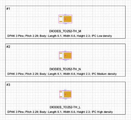
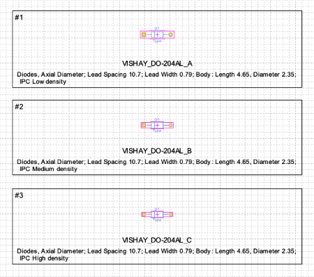
The different electronic products have different requirements of reliability, maintainability and density of the boards. With the 3-Tier footprint library construction concept, you can generate footprints to meet the different needs arising from component tolerances, the assembly process and the density of components on the board.
For each component, three geometric variants are provided for the pad dimensions and component profile: most material condition (low density, level A), nominal material condition (medium density, level B), least material condition (high density, level C).
The name of the footprint must end with a letter that identifies the level of belonging.
| Level | Description | Name suffix for SMD footprint | Name suffix for THD footprint |
|---|---|---|---|
|
Low density, level A |
For low density PCBs, the maximum pad size is used. |
M |
A |
|
Medium density, level B |
For medium density PCBs, the nominal pad size is used. |
N |
B |
|
High density, level C |
For high density PCBs, the minimum pad size is used. |
L |
C |
 Tip: Tip: |
|---|
For information on the 3-Tier PCB library, refer to the IPC-7351 standard. |
To create a 3-Tier footprint
-
Manually:
-
In the Page properties dialog you must activate the Symbols » The page describes an IPC footprint option.
Draw the footprint for density level A. See To draw a footprint.
Draw the footprint for density level B. See To draw a footprint.
Draw the footprint for density level C. See To draw a footprint.
-
-
Automatically:
For some families of components it is possible to create footprints automatically by specifying the dimensional parameters of the components. See Creating a footprint using the wizard.
All three footprints must reside on the same page.
 Note: Note: |
|---|
When you import a footprint from the libraries, the model corresponding to the construction level of the board, set in the parameter IPC Level in the dialog PCB Layer Stackup, is automatically selected. |
Example page for SMD component

Example page for THD component
